(China (Mainland))

Product Summary
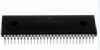
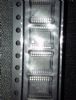
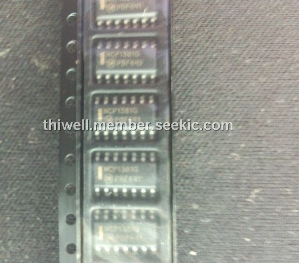
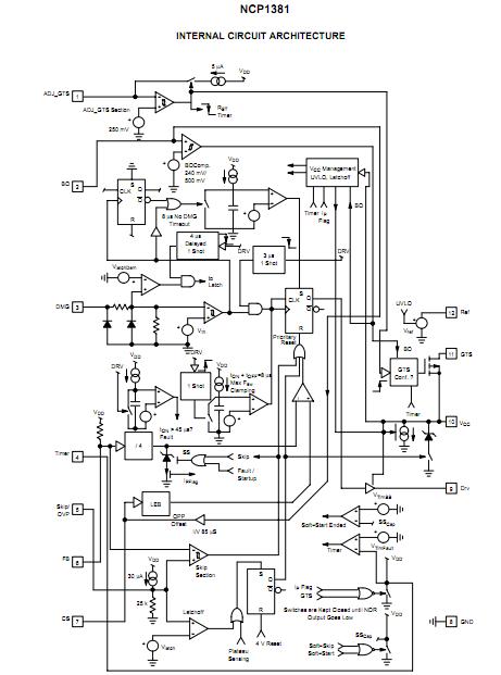
The NCP1381DR2G is a Low-Standby High Performance PWM Controller. Housed in a SO-14 package, the NCP1381DR2G includes everything needed to build rugged and efficient Quasi-Resonant (QR) Switching Power Supplies. When powered by a front-end Power Factor Correction circuitry, the NCP1381DR2G automatically disconnects the PFC controller in low output loading conditions (with an adjustable level), thus improving the standby power. Typical Applications of the NCP1381DR2G include High Power AC/DC Adapters for Notebooks, etc, Offline Battery Chargers and Set-Top Boxes Power Supplies, TV, Monitors, etc.
Parametrics
NCP1381DR2G absolute maximum ratings: (1)Vsupply, Maximum Power Supply Voltage on Pin 10 (VCC), Pin 9 (DRV), and Pin 11 (GTS): 20 V; Maximum Current in Pin 10 (VCC): ±30 mA; Maximum Current in Pin 11 (GTS): ±20 mA; Maximum Current in Pin 9 (DRV): ±1 A; (2)Power Supply Voltage on all Other Pins Except Pin 10 (VCC), Pin 9 (DRV), Pin 3 (DMG) and Pin 11 (GTS): -0.3 to 5 V; (3)Maximum Current Into All Other Pins Except Pin 10 (VCC), Pin 9 (DRV) and Pin 11 (GTS): ±10 mA; (4)Idem, Maximum Current in Pin 3 (DMG), When 10 V ESD Zener is Activated: +3 /-3 mA; (5)RθJ-A, Thermal Resistance Junction-to-Air: 150℃/W; (6)TJMAX, Maximum Junction Temperature: 150℃; (7)Storage Temperature Range: -60 to +150℃; (8)ESD Capability, Human Body Model: 2 kV; (9)ESD Capability, Human Body Model: 200 V.
Features
NCP1381DR2G features: (1)Current-Mode Quasi-Resonant Operation; (2)Adjustable Line Over Power Protection; (3)Extremely Low Startup Current of 15μA Maximum; (4)Soft-Skip Cycle Capability at Adjustable Peak Currents; (5)Plateau Sensing Overvoltage; (6)Brown-Out Protection; (7)Maximum tON Limitation; (8)Overpower Protection by current Sense Offset; (9)Internal 5 ms Soft-Start Management; (10)Short-Circuit Protection Independent from Auxiliary Level; (11)External Latch Input Pin for an OTP Signal; (12)Go-To-Standby Signal for the PFC Front Stage; (13)True Frequency (tON + tOFF) Clamp Circuit; (14)Low and Noiseless, No-Load Standby Power; (15)Internal Leading Edge Blanking; (16)+500 mA / -800 mA Peak Current Drive Capability; (17)5 V / 10 mA Reference Voltage; (18)This is a Pb-Free Device.
Diagrams
| Image | Part No | Mfg | Description |  |
Pricing (USD) |
Quantity | ||||||||||||
|---|---|---|---|---|---|---|---|---|---|---|---|---|---|---|---|---|---|---|
 |
 NCP1381DR2G |
ON Semiconductor |
Current Mode PWM Controllers ANA PWM CONTROLLER |
Data Sheet |
|
|
||||||||||||
| Image | Part No | Mfg | Description | |
Pricing (USD) |
Quantity | ||||||||||||
 |
NCP100 |
Other |
|
Data Sheet |
Negotiable |
|
||||||||||||
|
NCP1000 |
Other |
|
Data Sheet |
Negotiable |
|
||||||||||||
|
NCP1000P |
ON Semiconductor |
Other Power Management 700V 500mA Switching |
Data Sheet |
Negotiable |
|
||||||||||||
|
NCP1000PG |
ON Semiconductor |
Other Power Management 700V 500mA Switching w/OVP and Zero Duty |
Data Sheet |
Negotiable |
|
||||||||||||
|
NCP1001 |
Other |
|
Data Sheet |
Negotiable |
|
||||||||||||
|
NCP1001P |
ON Semiconductor |
Other Power Management 700V 500mA Switching |
Data Sheet |
Negotiable |
|
||||||||||||