(China (Mainland))

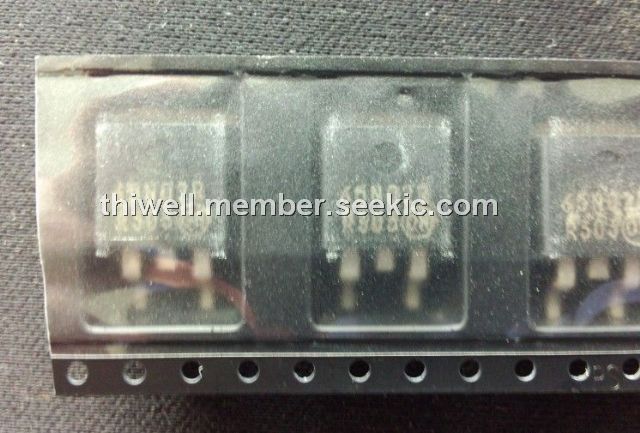
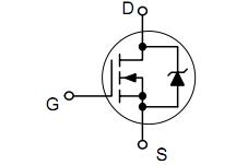
Product Summary
The 65N02R is a Power MOSFET.
Parametrics
65N02R absolute maximum ratings: (1)Drain-to-Source Voltage, VDSS: 25 Vdc; (2)Gate-to-Source Voltage - Continuous, VGS: ±20 Vdc; (3)Thermal Resistance, Junction-to-Case, RθJA: 67℃/W; (4)Total Power Dissipation @ TC = 25℃, PD: 62.5W; (5)Drain Current, ID: 65A; (6)Operating and Storage Temperature Range TJ and Tstg: -55 to; (7)150℃; (8)Single Pulse Drain-to-Source Avalanche, EAS: 60 mJ; (9)Maximum Lead Temperature for Soldering Purposes, 1/8" from Case for 10 Seconds, TL: 260℃.
Features
65N02R features: (1)Planar HD3e Process for Fast Switching Performance; (2)Low RDSon to Minimize Conduction Loss; (3)Low Ciss to Minimize Driver Loss; (4)Low Gate Charge; (5)Pb-Free Packages are Available.
Diagrams